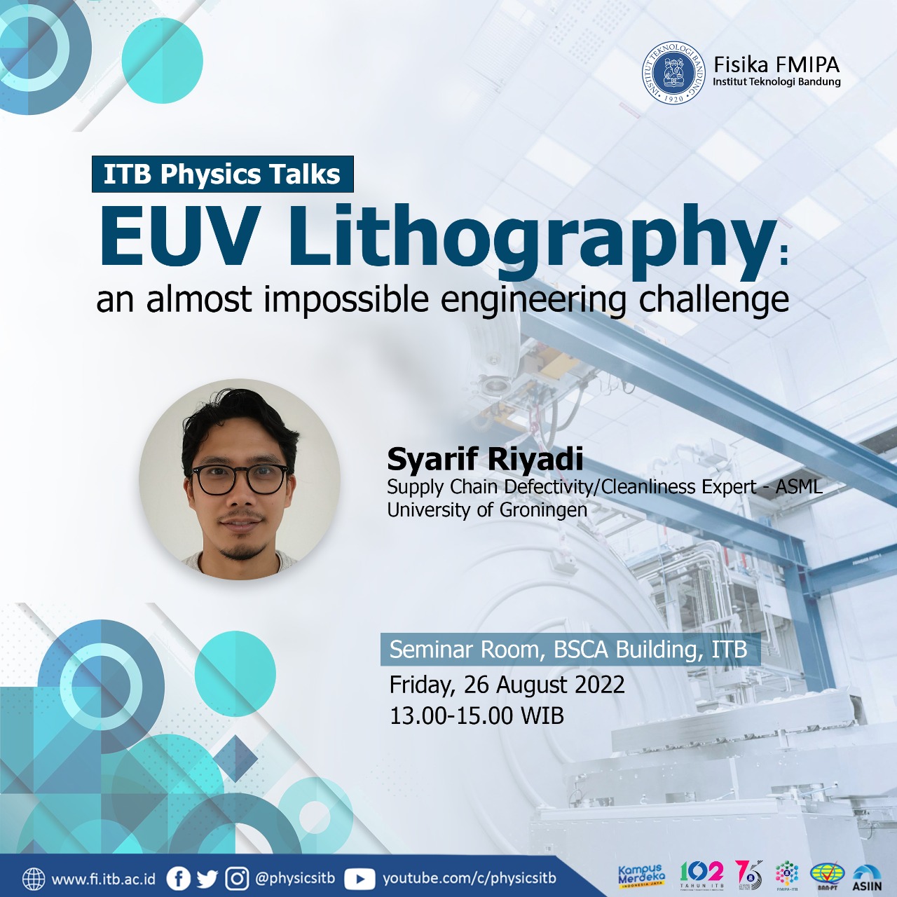
ITB PHYSICS TALKS
EUV Lithography: An Almost Impossible Engineering Challenge
Syarif Riyadi
Supply Chain Defectivity/Cleanliness Expert – ASML
University of Groningen
Friday, 26 August 2022, 13.00 WIB
Seminar Room, BSCA Building, ITB
Or you can attend online via Zoom:
https://itb-ac-id.zoom.us/j/99792628366?pwd=MmNzWXc5Rlo5OWdFMTA4b1dOU2dRUT09
Meeting ID: 997 9262 8366
Passcode: physics
Abstract
As one of many steps in semiconductor chips manufacturing process, lithography can be considered as the most crucial one. In the lithography process, the blue-print of the chips is ‘printed’ on the silicon wafer by high energy UV plasma. For example, to produce the existing electronic devices which use smaller transistor nodes, i.e. 5 or 7nm, an extreme UV (EUV) plasma at the wavelength of 13.5nm is used. The complete EUV lithography process make use of an extremely complex machine which involves multidiciplinary subjects, from simple to complex exotic physical phenomenon. A brief overview of the EUV lithography machine manufacturing chain and its crucial position in the current advancing digital world will be described.
Speaker’s Biography:
Education:
Bachelor – Fisika Material Elektronik, ITB (2003)
Master – Fisika Magnetik & Fotonik, ITB (2006)
Doctor – Solid State Materials for Electronics, Univ. Groningen, NL (2012)
Professional life:
– Senior Scientist R&D, Johnson Matthey Plc., NL (2012-2017)
– System Integrator, Canon Industrial Printing, NL (2017-2019)
– Supply Chain Defectivity Expert, ASML, NL (2020-now)
